Industries
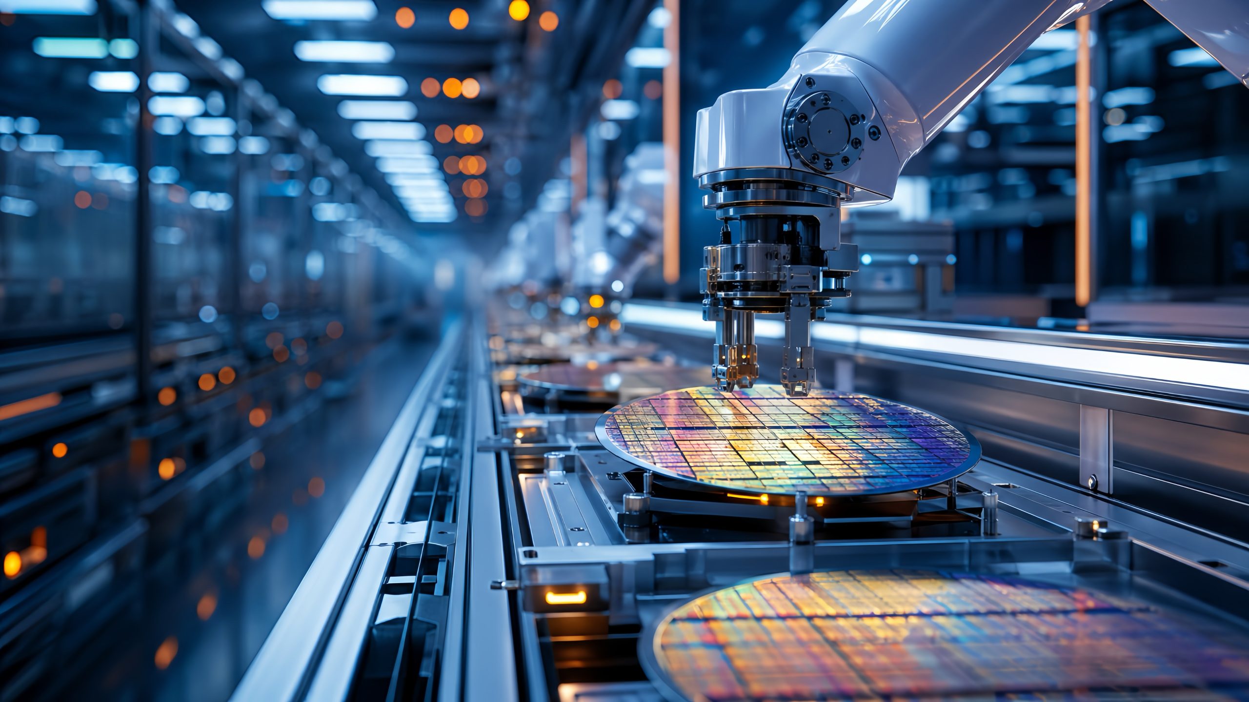
Semiconductor Materials and Process Solutions
Smaller features, new device architectures, and advanced packaging technologies are increasing the demands placed on semiconductor materials. Manufacturers must control purity, contamination, surface interactions, thermal behavior, and dimensional stability across multiple process stages.
Mitsubishi Chemical Group provides advanced materials, specialty chemicals, engineered components, and services from wafer manufacturing and front-end-of-line processing through back-end-of-line, packaging, power devices, and fab operations.
High-purity materials from the start
Contamination control begins before the wafer enters device fabrication. MCG supplies high-purity materials and processing technologies for silicon and compound-semiconductor wafer production.
Our capabilities include:
- Ultra-high-purity synthetic silica for quartz crucibles and components
- High-purity process chemicals and cleaning formulations
- Bulk GaN substrates for power, RF, optical, and electronic applications
- Wafer processing and reclaim services
Mitsubishi Synthetic Silica offers documented SiO₂ purity above 99.99999%, with individual measured metal impurities generally below 10–20 ppb.
- Deposition materials for controlled thin-film formation – Chemical vapor deposition (CLD) and atomic layer deposition (ALD) require precursors with suitable purity, volatility, thermal stability, and surface reactivity.
MCG and Gelest provide high-purity organometallic and organosilicon synthesis and precursor-development capabilities for CVD and ALD processes. - Materials for advanced lithography – Advanced patterning requires precise control over resist chemistry, precursor purity, molecular behavior, and film formation. High-NA EUV introduces further challenges involving absorption, dose, defectivity, and process control.
Our technologies include: Lithomax™ high-purity resist polymers for ArF and EUV lithography, aquaSAVE™ antistatic material for advanced photomask manufacturing, and Tin-based metal-organic precursors under development for CVD-deposited dry resist. - Cleaning and contamination control – Particles, metals and organic residues can interfere with contamination-sensitive wafer processes. MCG offers ultra-high-purity chemicals and formulated cleaning materials designed for specific process conditions.
MCG cleaning chemistry combines NH₄OH with chelating-agent technology to remove particles and organic residues while capturing metals and helping to prevent their rebinding to the wafer surface.
Materials for interconnect formation – Continued interconnect scaling creates demanding requirements for deposition, planarization, and post-CMP cleaning. MCG capabilities include:
- CVD and ALD precursors
- High-purity wet chemistry
- Post-CMP cleaning materials
- Engineered plastics for CMP equipment
Techtron™ engineering plastic is used in CMP retaining-ring applications requiring mechanical and dimensional performance during repeated chemical and mechanical exposure.
Balancing thermal expansion, flow and processability
Chiplets, hybrid bonding, wafer-level packaging, panel-level packaging, and 3D integration bring multiple materials together within increasingly dense structures. This makes thermal expansion, viscosity, adhesion, insulation, and heat transfer critical considerations.
MCG technologies include:
- Spherical negative-thermal-expansion fillers for underfill and molding compounds
- jER™ epoxy resins for insulation, adhesion, and encapsulation
- Ultra-thin thermally conductive films under development
- DIAFOIL™ functional films for dicing and packaging
- Non-fluorinated polyester mold-release films under development for wafer- and panel-level packaging
In experimental evaluation and capillary-flow simulation, MCG’s surface-treated NTE filler demonstrated lower CTE with practical viscosity and filling of a 50 μm gap.
- Selective wet etching for Si and SiGe structures – Backside power delivery network integration requires silicon removal while preserving increasingly thin SiGe etch-stop layers.
MCG has developed an engineered alkaline Si/SiGe wet etchant that achieved approximately 750 selectivity in full 12-inch single-wafer processing, compared with approximately 160 for conventional chemistry. - Power semiconductor materials – Power devices require careful management of substrate quality, heat, electrical insulation, and high-temperature operating conditions.
MCG provides:- Bulk GaN substrates produced using HVPE and ammonothermal technologies
- Electrically insulating thermal materials
- Thermally conductive films
- Materials for power-electronics components and assemblies
Equipment components must perform under aggressive chemical exposure, mechanical wear, and strict contamination controls.
MCG supplies engineered plastics, carbon-fiber composites and functional polymers for wafer handling, CMP equipment, semiconductor transport, and structural components.
DIALEAD™ pitch-based carbon-fiber end effectors combine high stiffness and low weight with vibration damping, Electrostatic Dissipation (ESD) control, chemical resistance, and near-zero axial Coefficient of Thermal Expansion (CTE).
MCG Group capabilities also support semiconductor manufacturing infrastructure through:
- Wafer reclaiming and processing
- Precision equipment cleaning
- Ultrapure-water production
- Wastewater treatment and recycling
- Chemical supply and recovery systems
Develop your next semiconductor material
From materials design and analytical evaluation to process integration, scale-up, and manufacturing, MCG works with semiconductor manufacturers, equipment companies, and ecosystem partners on established and emerging requirements.